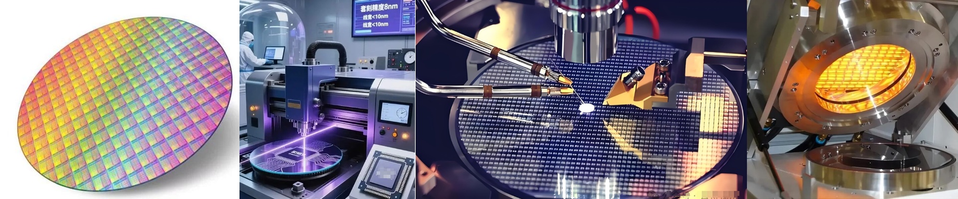

Why we use IR Curing for Lead-Free Semiconductor Standards
When people talk about “going green” or “lead-free” in wafer tool design, they usually focus on the chemicals. But here’s the thing: it’s actually more about how you handle the heat. That’s why we lean on infrared (IR) curing. Instead of trying to bake the entire tool chamber, we just target the substrate.
Getting the heat where it actually matters
Think about a standard convection oven. It spends way too much time just heating up the air. It’s a waste. IR is different. It uses electromagnetic radiation to get the molecules in the adhesive or photoresist moving. The result? Your wafer hits the right temperature in seconds. You aren’t fighting the bulk of the machine, which is exactly why IR has become the go-to for saving energy in the cleanroom.
Staying in that “sweet spot”
Lead-free polymers and solders are picky. They have a very tight thermal window. If you go too hot, you’re looking at warped wafers or permanent damage. It’s a nightmare. To stop that from happening, we build precision sensors right into the tool to keep an eye on those temperature peaks as they happen. Because we use short-wave IR, we can crank the heat up or kill it instantly. It’s a level of control you just don’t get with slow, bulk-heating methods that tend to degrade the chemicals.
The trade-off (because there’s always one)
IR is fast. Really fast. But that speed comes with a catch. The heat density is intense. If your sensors are in the wrong spot or your PID loop isn’t tuned just right, you’ll end up with hot spots across the wafer. Plus, you’ve got to make sure your cooling system can keep up with that rapid cycling, or you’ll fry your sensors. We’ve found that the magic happens when you pair IR emitters with high-frequency sensors. It keeps everything within those strict environmental limits without needing any of those old, toxic heating agents.